
Understanding Gerber Files: A Comprehensive Guide for PCB Designers
Gerber files are an essential component in the world of printed circuit board (PCB) design. As a PCB designer, you need to have a deep understanding of these files to ensure the successful production of your PCBs. In this article, we will delve into the intricacies of Gerber files, covering their purpose, structure, and how to work with them effectively.
What are Gerber Files?

Gerber files are a set of files that contain the design data for a PCB. They are used by PCB manufacturers to produce the actual boards. These files are created using Gerber software, which is specifically designed for PCB design and manufacturing.
Gerber files are typically in the .gbr or .gbr.gz format. They contain information about the layers of the PCB, including the copper layers, soldermask, silk screen, and drill holes. Each layer is represented by a separate file, and the files are usually organized in a specific directory structure.
Understanding the Structure of Gerber Files
The structure of a Gerber file is quite complex, but it is essential to understand it to work with these files effectively. Here is a breakdown of the key components:
| Component | Description |
|---|---|
| Header | Contains metadata about the file, such as the format version, units of measurement, and the number of layers. |
| Plot Area | Describes the area of the PCB that is to be plotted. This includes the origin, size, and orientation of the PCB. |
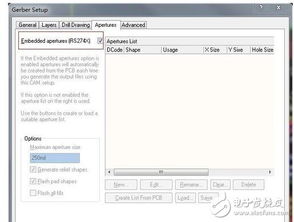
| Aperture Definition | Describes the shapes and sizes of the apertures used to create the PCB layers. Apertures can be circles, rectangles, or polygons. |
| Aperture Usage | Specifies which apertures are used for each layer of the PCB. For example, a copper layer might use a circle aperture for the copper pads, while a soldermask layer might use a rectangle aperture for the soldermask. |
| Plot Data | Contains the actual data that is to be plotted on the PCB. This includes the positions and sizes of the copper traces, vias, and other components. |
Understanding the structure of Gerber files is crucial for ensuring that the PCB is manufactured correctly. Any errors in the Gerber files can lead to manufacturing issues, such as short circuits or missing components.
How to Work with Gerber Files
Working with Gerber files involves several steps, from creating the files to verifying their accuracy. Here is a step-by-step guide:
-
Create the PCB design using PCB design software such as Altium Designer, Eagle, or KiCad.
-
Export the design as Gerber files. Most PCB design software has a built-in export function that generates the necessary Gerber files.
-
Verify the Gerber files using a Gerber viewer. This will help you identify any errors or issues in the files.
-
Send the Gerber files to the PCB manufacturer. Ensure that you provide all the necessary files and documentation, such as the drill file and assembly drawing.
-
Review the PCB after manufacturing to ensure that it meets your design specifications.
Common Issues with Gerber Files
Despite the importance of Gerber files, there are several common issues that can arise during the design and manufacturing process. Here are some of the most common problems:
-
Missing Layers: Ensure that all layers are included in the Gerber files, as missing layers can lead to manufacturing errors.
-
Incorrect Aperture Definitions: Verify that the apertures used for each layer are correct, as incorrect apertures can cause manufacturing issues.
-
Overlapping Traces: Check for overlapping traces, as this can lead to short circuits or other electrical issues.
-
Improper Layer Stackup: Ensure that the layer stack


